- 您现在的位置:买卖IC网 > Sheet目录3753 > ATMEGA169P-16MCHR (Atmel)MCU AVR 16KB FLASH 16MHZ 64-VQFN
2005 Microchip Technology Inc.
Preliminary
DS41265A-page 239
PIC16F946
19.6
AC Characteristics: PIC16F946 (Industrial, Extended)
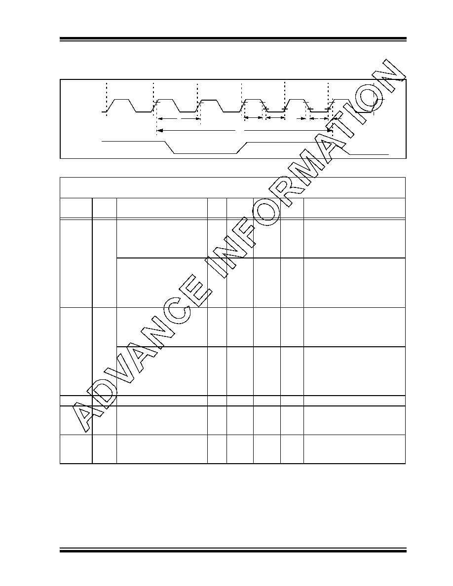
FIGURE 19-3:
EXTERNAL CLOCK TIMING
TABLE 19-1:
EXTERNAL CLOCK TIMING REQUIREMENTS
Standard Operating Conditions (unless otherwise stated)
Operating Temperature
-40°C
≤ TA ≤ +125°C
Param
No.
Sym
Characteristic
Min
Typ
Max
Units
Conditions
FOSC
External CLKI Frequency(1)
DC
—
37
kHz
LP Oscillator mode
DC
—
4
MHz
XT Oscillator mode
DC
—
20
MHz
HS Oscillator mode
DC
—
20
MHz
EC Oscillator mode
Oscillator Frequency(1)
5
—
37
kHz
LP Oscillator mode
—
4
—
MHz
INTOSC mode
DC
—
4
MHz
RC Oscillator mode
0.1
—
4
MHz
XT Oscillator mode
1
—
20
MHz
HS Oscillator mode
1TOSC
External CLKI Period(1)
27
—
∞μs
LP Oscillator mode
50
—
∞
Ns
HS Oscillator mode
50
—
∞
ns
EC Oscillator mode
250
—
∞
ns
XT Oscillator mode
Oscillator Period(1)
27
200
μs
LP Oscillator mode
—
250
—
ns
INTOSC mode
250
—
ns
RC Oscillator mode
250
—
10,000
ns
XT Oscillator mode
50
—
1,000
ns
HS Oscillator mode
2TCY
Instruction Cycle Time(1)
200
TCY
DC
ns
TCY = 4/FOSC
3TosL,
TosH
External CLKI (OSC1) High
External CLKI Low
2*
—
μs
LP oscillator, TOSC L/H duty cycle
20*
—
ns
HS oscillator, TOSC L/H duty cycle
100 *
—
ns
XT oscillator, TOSC L/H duty cycle
4TosR,
TosF
External CLKI Rise
External CLKI Fall
—
50*
ns
LP oscillator
—
25*
ns
XT oscillator
—
15*
ns
HS oscillator
*
These parameters are characterized but not tested.
Data in ‘Typ’ column is at 5V, 25°C unless otherwise stated. These parameters are for design guidance
only and are not tested.
Note 1:
Instruction cycle period (TCY) equals four times the input oscillator time base period. All specified values
are based on characterization data for that particular oscillator type under standard operating conditions
with the device executing code. Exceeding these specified limits may result in an unstable oscillator
operation and/or higher than expected current consumption. All devices are tested to operate at ‘min’
values with an external clock applied to OSC1 pin. When an external clock input is used, the ‘max’ cycle
time limit is ‘DC’ (no clock) for all devices.
OSC1
CLKO
Q4
Q1
Q2
Q3
Q4
Q1
1
2
3
4
发布紧急采购,3分钟左右您将得到回复。
相关PDF资料
2-1546217-0
TERM BLK RCPT 20POS SIDE 5.08MM
1-1546217-9
TERM BLK RCPT 19POS SIDE 5.08MM
1-1546217-8
TERM BLK RCPT 18POS SIDE 5.08MM
1-1546217-7
TERM BLK RCPT 17POS SIDE 5.08MM
1-1546217-6
TERM BLK RCPT 16POS SIDE 5.08MM
1-1546217-5
TERM BLK RCPT 15POS SIDE 5.08MM
1-1546217-4
TERM BLK RCPT 14POS SIDE 5.08MM
1-1546217-3
TERM BLK RCPT 13POS SIDE 5.08MM
相关代理商/技术参数
ATMEGA169P-16MCU
功能描述:8位微控制器 -MCU AVR 16KB, 512B EE 16MHz 1KB SRAM, 5V
RoHS:否 制造商:Silicon Labs 核心:8051 处理器系列:C8051F39x 数据总线宽度:8 bit 最大时钟频率:50 MHz 程序存储器大小:16 KB 数据 RAM 大小:1 KB 片上 ADC:Yes 工作电源电压:1.8 V to 3.6 V 工作温度范围:- 40 C to + 105 C 封装 / 箱体:QFN-20 安装风格:SMD/SMT
ATMEGA169P-16MU
功能描述:8位微控制器 -MCU AVR 16K FLASH 512B EE 1K SRAM LCD ADC RoHS:否 制造商:Silicon Labs 核心:8051 处理器系列:C8051F39x 数据总线宽度:8 bit 最大时钟频率:50 MHz 程序存储器大小:16 KB 数据 RAM 大小:1 KB 片上 ADC:Yes 工作电源电压:1.8 V to 3.6 V 工作温度范围:- 40 C to + 105 C 封装 / 箱体:QFN-20 安装风格:SMD/SMT
ATMEGA169P-16MU SL383
制造商:Atmel Corporation 功能描述:MCU 8BIT ATMEGA RISC 16KB FLASH 3.3V/5V 64PIN MLF - Tape and Reel
ATMEGA169P-16MUR
功能描述:8位微控制器 -MCU AVR LCD 16KB FLSH EE 512B 1KB SRAM-16MHZ RoHS:否 制造商:Silicon Labs 核心:8051 处理器系列:C8051F39x 数据总线宽度:8 bit 最大时钟频率:50 MHz 程序存储器大小:16 KB 数据 RAM 大小:1 KB 片上 ADC:Yes 工作电源电压:1.8 V to 3.6 V 工作温度范围:- 40 C to + 105 C 封装 / 箱体:QFN-20 安装风格:SMD/SMT
ATMEGA169P-8AU
制造商:ATMEL 制造商全称:ATMEL Corporation 功能描述:Microcontroller with 16K Bytes In-System Programmable Flash
ATMEGA169P-8MU
制造商:ATMEL 制造商全称:ATMEL Corporation 功能描述:Microcontroller with 16K Bytes In-System Programmable Flash
ATMEGA169PA
制造商:ATMEL 制造商全称:ATMEL Corporation 功能描述:8-bit Microcontroller with 16K Bytes In-System Programmable Flash
ATMEGA169PA_1
制造商:ATMEL 制造商全称:ATMEL Corporation 功能描述:High Endurance Non-volatile Memory segments